

Heavy Copper PCBs Reduce Voltage
Printed circuit boards (PCBs) are essential to many electronic systems, but they require careful engineering and fabrication to ensure optimal quality. One of the most important considerations is voltage drop in circuits, which can impact signal integrity and cause other issues. Heavy copper PCBs can reduce this issue by enhancing current-carrying capacity and enabling efficient thermal management.
The PCB fabrication process begins with a design, specified using a CAD software program. The design specifies the layers of the board, and where components are placed. It also includes holes, known as vias, that connect the layers of the board. The size and location of the vias are determined by the PCB design, as well as the copper thickness.
Once the design has been approved, the substrate material, typically a fiberglass like FR-4, is prepped and pre-coated with a thin layer of copper. The copper is then etched, and holes are drilled into the board for component leads. The drilled holes are then filled with copper, creating the vias. The copper thickness in a heavy copper pcb is typically much thicker than a standard PCB, which can lead to some challenges when it comes to etching and plating.
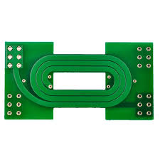
Heavy Copper PCBs Reduce Voltage Drop in Circuits
The thicker copper in a heavy copper PCB helps to mitigate issues such as skin effect and impedance at high frequencies. The increased copper thickness also provides better heat dissipation, allowing the conductor to operate at its optimal temperature without risking overheating or excessive voltage drops. This benefit is especially important in power-intensive applications.
In addition to the improved current-carrying capability and thermal management offered by heavy copper, these boards offer enhanced mechanical strength. The increased copper mass is less susceptible to cracking or delamination, which makes them more durable and rugged for use in demanding environments.
However, there are some significant manufacturing hurdles that must be overcome when designing a heavy copper PCB. Specialized etching and plating processes are required to work with this thickness, and the board fabricator must be careful to prevent voids in the copper.
The construction of heavy copper PCBs involves advanced manufacturing techniques tailored to accommodate the increased copper thickness. During the fabrication process, specialized equipment and materials are employed to deposit thick copper layers onto the substrate, ensuring uniform distribution and adherence. Additionally, the substrate material itself is often selected for its high thermal conductivity and mechanical strength to withstand the demands of high-power applications.
Drilling and hole sizes must be carefully considered, as the copper thickness may necessitate specialized drilling techniques to achieve accurate results. Furthermore, it is important to collaborate with an experienced manufacturer and follow the appropriate design guidelines when working with a heavy copper PCB. This will help to minimize any unforeseen issues during the production process. Lastly, the cost of producing a heavy copper PCB can be higher than that of a standard PCB due to the additional materials and processing steps required.


